Two
- Analog
- 2023-09-23 21:19:17
Schemes of two-half-period rectifiers on op amps with switching inputs in accordance with the polarity of the input voltage are given. The switching of inputs is performed by a control signal taken from the output of the zero-indicator made on the comparator.
Precision two-half-period rectifiers, whose operation is based on switching inputs in accordance with the polarity of the input voltage, usually contain an op amp, the non-inverting input of which is shunted by a diode, Figure 1, R1 = R2 = 2R3.
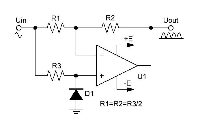
Figure 1 Classical scheme of a precision two-half-period rectifier.


Wow the engineering world with your unique design: Design Ideas Submission Guide
When a positive half-wave of the input voltage enters the input, the diode D1 is locked. The op amp U1 operates in the mode of a non-inverting amplifier with a transmission coefficient equal to R2/R1. The output voltage is equal to the input voltage: Uout = Uin.
When a negative half-wave of the corresponding amplitude arrives at the input of the device, the diode D1 opens, the circuit operates in the mode of an inverting amplifier with a transmission coefficient equal to –1, Uout = –Uin.
The disadvantage of the circuit is obvious: with a low input voltage of negative polarity due to the fact that the diode D1 has a noticeable resistance, Uout ≠ –Uin. In practice, the amplitude of the input signal when using the op amp U1 LM324 and the diode D1 1N4148 should be in the range of 2.5 V to the supply voltage.
It is possible to improve the operation of a precision two-half-period rectifier by using key elements (FET Q1, Figure 2, or analog switch U2, Figure 3), controlled by a zero detector on the comparator U1.1.
The practical scheme of the first of the devices is shown in Figure 2.

Figure 2 A two-half-period rectifier with switching of the input of an op amp by a FET.
A zero detector of the input signal is made on the comparator U1.1 of the LM339 chip. From the output of this detector, the control signal is applied to the gate of the FET Q1 2N3823, which switches the input of the op amp U2.1 of the LM324 chip.
The amplitude of the input signal when using an op amp U2.1 LM324 and a FET Q1 2N3823 should be in the range of 0.5 V from the supply voltage.
It is possible to improve a two-half-period rectifier by using an analog U3 switch as a switching element such as Figure 3, for example, CD4066, or a more modern element with less losses. To reduce the resistance of the public key, all 4 channels of the CD4066 switch should be connected in parallel. The switch S1 can change the polarity of the output signals.

Figure 3 A two-half-period rectifier with switching of the input of an op amp by an analog switch.
The precision of the two-half-period rectifier in Figure 3 is operable in the input voltage range from 20 mV to the supply voltage of the device. The maximum frequency of the rectifier is 100 kHz and depends on the frequency properties of the active elements.
Michael A. Shustov is a doctor of technical sciences, candidate of chemical sciences and the author of over 750 printed works in the field of electronics, chemistry, physics, geology, medicine, and history.
Related Content
AC comparator with color-dynamic signal level indicationGenerate boost rails in a bridge-rectifier circuitCapacitor capacity comparatorInductance comparatorBinary elements of fractional logicTwo由Voice of the EngineerAnalogColumn releasethank you for your recognition of Voice of the Engineer and for our original works As well as the favor of the article, you are very welcome to share it on your personal website or circle of friends, but please indicate the source of the article when reprinting it.“Two”