A Motorola Nexus 6 teardown
- 5G
- 2023-09-23 20:18:56
This article explores the internal makings of a Motorola Nexus 6 cellphone with a focus on components relevant to cellular telecommunication, including an RF transceiver, cellular modem, and Wi-Fi/Bluetooth ICs. I also outline the step-by-step process used to access the inside of the cellphone. A video of this teardown can be viewed here:
Removing the back cover
The first step in reaching the internals of the Nexus 6 is removing the backplate which is attached with a line of adhesive around the back perimeter of the phone. The tools used are:


Using the flathead screwdriver, pry open a corner of the back cover, allowing just enough room for the tip of the guitar pick to enter. Then shimmy the guitar pick along the edges of the back cover, levering it upwards to separate the line of adhesive connecting the back cover to the phone. I left the screwdriver in its original position to keep the corner wedged open in case the guitar pick slipped out during this step. Once roughly half of the back cover was separated, there was enough leverage to simply pry off the rest of the back cover by hand. I found the back cover to be pretty indelicate, so I could apply considerable force to separate the cover.
With the back cover removed, the back frame is visible now, containing the induction coil and battery.
Opening the back frame
Along the edges of the back frame and next to the camera lens should be twenty-two (22) T3 Torx screws. Undo these screws to separate the back frame from the screen and motherboard (Figure 1). (The tool used for this was a T3 Torx Screwdriver.)

Separating the motherboard from the screen
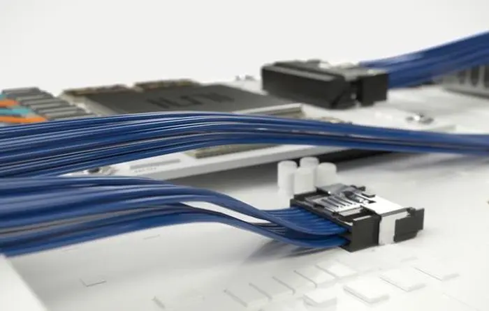
As shown in Figure 2, there are two ribbon cables which connect the screen to the motherboard; the first and larger one is the display cable, responsible for relaying video information from the motherboard to the screen; and the second is the touch screen cable that feeds touchscreen inputs to the rest of the phone.

Figure 2 Location of video (red) and touchscreen (blue) ribbon cable connectors.
Both ribbon cables’ connectors are located underneath Kapton tape. To remove the display cable, locate the long ribbon connected below and to the left of the back-facing camera (highlighted red in the above diagram). Using an anti-static spudger, lift the thin white bar opposite the ribbon. Then, you can pull the ribbon away from the connector with tweezers or the spudger.
The touchscreen input cable can be released by similarly lifting up the black tab on its respective connector (highlighted blue). Then again free the ribbon from its connector with the tweezers.
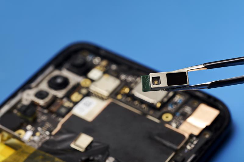
Removing IC shielding
With the motherboard separated, the last thing preventing direct inspection of the ICs are the silver IC shields. Removing these shields should be avoided unless accessing the ICs on the motherboard is necessary for repair or observation; the methodology to remove these shields without dedicated tools can damage the components underneath and renders the shields unusable for replacement. The tools used for this step were tweezers, a heat gun, safety goggles, and a soldering helping hand. Note the safety goggles were very helpful when stray solder, or fragments of IC shielding flung off the board as the shield was freed from the board.
The motherboard was firmly placed in the helping hands and tightened to maximize resistance against any forces applied to the board. I inserted the tweezers into one of the holes in the top of the shield, preferring holes at the corners and choked upwards on the tweezers, away from the shield to prevent burns, and apply a constant upwards force, either by levering downwards or pulling directly upwards.
The heat gun was placed closely above the perimeter of the IC shield (anything more than a few millimeters above the motherboard may mean the solder may not get sufficient heat to melt) and I began travelling the perimeter of the shield, heating all sides equally. If the shield is small enough, you may begin to feel the shield beginning to loosen; continue pulling upwards with the tweezers and walking the perimeter of the shield with the heat gun and the IC should come completely free in one motion.
Telecommunication ICsThis report is primarily focused on the cellular telecommunications aspect of the Nexus 6 so the first and most extensive section will be placed on ICs relevant to this area. However, other ICs will still be briefly touched upon, categorized into whether the IC has a “primary” or “auxiliary” role to the phone’s function. Figure 3 highlights the cellular ICs within the Nexus 6.

Figure 3 An outline of the telecommunication ICs in the Nexus 6.
Broadcom BCM4356 802.11ac + Bluetooth 4.1 IC
The BCM4356 is a highly integrated single-chip device that provides high speed wireless communication over Wi-Fi and Bluetooth. For Wi-Fi, the chip supports IEEE 802.11ac, as well as more legacy IEEE 802.11 protocols. The chip uses spatial multiplexing to transmit/receive using multiple antennae and can support up to 867 Mbps of data. This high data rate is achieved with the chip’s support of 256 QAM over an 80 MHz channel, allowing a single modulation symbol to encode an entire byte of information.
In addition, the BCM4356 supports IEEE 802.15.2, a Wi-Fi protocol which seeks to minimize interference between wireless networks operating in the same or nearby frequency bands. Although the protocol was originally built to mitigate interference between similarly banded IEEE 802.11 protocols, the BCM4356 datasheet suggests the IEEE 802.15.2 protocol is used to mitigate the interference between Wi-Fi and LTE/GPS.
The Bluetooth module in the BCM4356 supports Bluetooth 4.1, the most recent iteration of Bluetooth at the time. The BCM4356 also advertises its support for extended Synchronous Connections (eSCO) to improve link reliability and for adaptive frequency hopping (AFH) to mitigate collisions/interference is busy frequency bands. Both these features were introduced in Bluetooth 1.2. Another interesting feature of the BCM4356 is that it contains hardware support for various authentication and encryption, including WPA/WPA2 and AES.
Qualcomm MDM9625M LTE Modem
Through a cellular telecommunications lens, this IC is the most important component of the phone. Released in 2012, this cellular modem provided LTE Advanced capabilities to the smartphones of its time, including the iPhone 6 generation and this Nexus 6 model. Also referred to as 3GPP Release 10, LTE Advanced offered twice the user throughput when compared to prior LTE releases. It could support a peak downlink data rate of 1 Gbps and an uplink of 500 Mbps; the MDM962M doesn’t, however, capitalize on this—only offering data rates up to a still respectable 150 Mbps.
Texas Instruments TMS320C5545 Digital Signal Processor (DSP)
The TMS320C55 is a general-purpose DSP unit. It is highly programmable and can be tailored to many different applications. Some of the applications suggested by its datasheet include audio control, biometrics, voice applications, and software-defined radio; within the context of the Nexus 6, it is likely that this IC is used for one or both of the latter two applications. However, because RF telecommunications are covered in more depth with other ICs, we will focus on the possibility of voice encoding for the TMS320C5545.
A paper by Yang et al. demonstrates that the adaptive multi-rate (AMR) codec can be implemented very efficiently on a very similar DSP unit, the TMS320C64X [1]. Yang et al. tailor the AMR codec approach to be more efficiently ran on DSPs by introducing more parallelism with double ping-pong buffers and by improving memory locality. Because their paper was written in 2008, much before the widespread adoption of Voice-over-LTE (VoLTE) and adaptive multi-rate wideband (AMR-WB), Yang et al. only demonstrates using a DSP with AMR bitrates up to 12.2 kbps. However, with a clock speed up to 100 MHz, AMR-WB—with rates up to 23.85 kbps—could easily be supported by the TMS320C5545; this is strengthened by the fact that VoLTE support was added to the Nexus 6 in 2015 [2].
WCD9320 OVV Audio Codec IC
Although this component is referred to as a “audio codec” in its documentation (more accurately, the WCD9335’s documentation), it doesn’t appear to be responsible for the voice encoding responsible for making phone calls. Instead, the WCD9320 is responsible for preprocessing audio inputs, post processing audio outputs, and multiplexing/routing signals to the correct destination. Within its digital processing block diagram are arrays of multiplexors, mixers, decimators, interpolators, and high pass filters to adjust incoming/outgoing audio signals.
Qualcomm WTR1625L RF Transceiver
Transceivers, like the WTR1625L, are responsible for providing the physical interface through which cellular and other RF signals are received and transmitted. The WTR1625L was built to support the transition to LTE Advanced as it is the first transceiver IC the cellular industry to “support carrier aggregation with a significant expansion in the number of active RF bands”. The WTR1625L still supports previous cellular generations, namely 2G and 3G, and also accommodates GPS, including GLONASS and Beidou signals.
Qualcomm WFR1620 receive-only companion chip
Although documentation on the WFR1620 is sparse, some vendors suggest that the WFR1620 acts as a post-processing unit to the WTR1625L, performing the necessary operations to multiplex and interpret signals from multiple carriers received by the WTR1625L to implement carrier aggregation.
Qualcomm QFE1100 envelope tracking IC
The QFE1100 is responsible for the calculations involved in envelope tracking, a practice to improve the efficiency of the power amplifiers used to transmit signals [3]. The envelope of an AC signal is a smooth curve generalizing the signal’s peaks. Envelope tracking adjusts the voltage supplied to the power amplifier in real-time based on the envelope of the signal being transmitted, ensuring that the amplifier operates at peak efficiency. Where a fixed amplifier supply would generate power losses in the form of heat, applying envelope tracking provides significant power savings, improved battery life for mobile devices, and reduced heat generation. Because of the QFE1100’s function, it likely has a direct interface with the RF7389EU F14NRC2 power amplifier.
RF Micro Devices RF7389EU F14NRC2 envelope tracking power amplifier
The RF7389EU F14NRC2 is a power amplifier that supports envelope tracking (See QFE1100).
Primary function ICsThis section focuses on ICs that perform “primary” functions. Figure 4 outlines two of these ICs.

Figure 4 Outline of primary function ICs in the Nexus 6.
SK Hynix H9CKNNNDBTMTAR 3 GB LPDDR3 RAM with Qualcomm Snapdragon 805 SoC
The largest IC, which seems to dominate the center of the motherboard is the CPU/RAM combination chip. The onboard RAM is a 3 GB LPDDR RAM chip built into the processor, communicating with the CPU over two channels at 800 MHz.
The CPU, the Qualcomm Snapdragon 805 SoC, is specifically built for personal cellular devices. As such, its specifications list interfaces for cellular and Wi-Fi modems. Its cellular interface supports downlink speeds up to 300 Mbps and uplink speeds of 50 Mbps. This interface is a bottleneck, as the LTE modem in the Nexus 6, the Qualcomm MDM9625M, supports 1 Gbps and 500 Mbps downlink and uplink respectively. However, the cellular interface is LTE Category 6, meaning it is the first category to support LTE Advanced.
The Snapdragon’s Wi-Fi interface supports data rates of 867 Mbps with spatial multiplexing and channel rates of up to 80 MHz with a maximum of 256 QAM. Specifications that match the BCM4356 Wi-Fi and Bluetooth modem exactly.
SanDisk SDIN9DW4-32G 32 GB eMMC NAND flash
This IC, the SDIN9DW4, is responsible for the non-volatile memory of the Nexus 6. It stores up to 32 GB and has a data rate of 400 MB/sec.
Auxiliary Function ICsThis section focuses on ICs that perform “auxiliary” functions. Figure 5 highlights the ICs that perform these functions.

Figure 5 Outline of auxiliary function ICs within the Nexus 6.
TFA9890A audio amplifier
The TFA9890A is a voltage booster, amplifying the 3.6 V supply voltage of the cellphone battery up to 9.5 V to drive speakers. There are two, located near the top and bottom speakers of the Nexus 6.
BCM20795P1KML1G NFC chip
The BCM20795P1KML1G is a near field communication (NFC) controller chip manufactured by Broadcom. It enables NFC communication between devices in proximity, typically within a few centimeters. Although no datasheets are readily available for this specific chip, it is likely that this IC supports the ISO/IEC 14443 and FeliCa NFC protocols, handling short range, secure, data transmissions.
Qualcomm SMB1359
The SMB1359 is a programmable high-capacity LiPo battery charger. It includes a sundry of safety features, including overcurrent & over/undervoltage safeguards, watchdog timers, charge current/float voltage compensation, and thermal protection. Able to charge a LiPo battery at up to 2.6 A, and supports USB TurboCharge mode.
Michael Fuhrer is a Master’s of Computer Engineering student atVirginia Tech.
Related Content
Teardown: Inside the iPhone 6 PlusVoIP phone teardownDisassembling a “dumb phone”Teardown: Cell-phone charger: nice idea done rightDisassembling a wireless charger with a magnetic personalityUngluing a GaN chargerReferences
Jie Yang, Sheng sheng Yu and Mian Zhao, “The implementation and optimization of AMR speech codec on DSP,” 2007 International Symposium on Intelligent Signal Processing and Communication Systems, Xiamen, 2007, pp. 365-367, doi: 10.1109/ISPACS.2007.4445899.Kellen, “Tip: Simultaneous voice and data now works on Nexus 6 with Verizon,” Droid Life, 12-Mar-2015. [Online]. Available: https://www.droid-life.com/2015/03/12/tip-simultaneous-voice-and-data-now-works-on-nexus-6-with-verizon/. [Accessed: 30-Apr-2023].G. Wimpenny, “Improving multi-carrier PA efficiency using envelope tracking,” EE Times, 02-Mar-2008. [Online]. Available: https://www.eetimes.com/Improving-multi-carrier-PA-efficiency-using-envelope-tracking/. [Accessed: 28-Apr-2023].A Motorola Nexus 6 teardown由Voice of the Engineer5GColumn releasethank you for your recognition of Voice of the Engineer and for our original works As well as the favor of the article, you are very welcome to share it on your personal website or circle of friends, but please indicate the source of the article when reprinting it.“A Motorola Nexus 6 teardown”