A deep dive inside a USB flash drive
- Consumer
- 2023-09-23 22:51:38
More than two years ago, within my review of a premium portable audio player, I told the tale of acquiring two claimed 400 GByte microSD flash memory cards that ended up not being even close to what the merchant claimed from a true-capacity standpoint. At the time I had my own “fake” experience, I was already aware that shenanigans sometimes occurred in the microSD card world, spoofing not only the amount of available storage but also the manufacturer. And I’ve subsequently learned that such trickery isn’t restricted solely to memory cards; coverage from mid-last year showcased a scam involving a portable SSD supposedly 30 TBytes in size for only $39, which fooled mighty Walmart (to the subsequent dismay of the retailer’s customers).
At the time, I’d mentioned I’d added the two fake-capacity microSD cards to my teardown pile for later revisit. “Later” ended up being the Christmas 2022 holidays. And as for “teardown”, well, I tried. Here are some briefly-back-in-retail-packaging shots of the microSD shysters and their associated SD card adapters (whose functionality I haven’t tested, come to think of it):
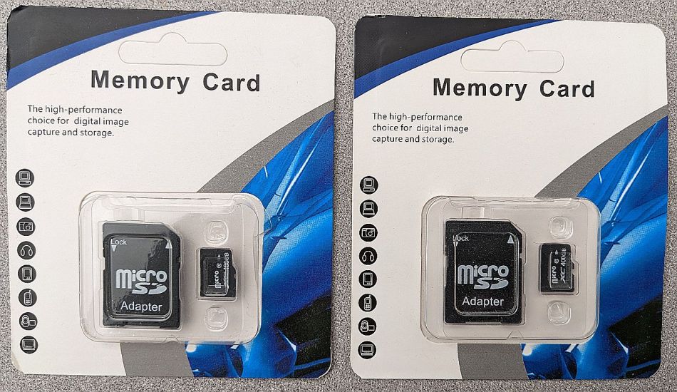

They look reasonably legit, right? Right…now here’s a closer look at ‘em out of the packaging:


At that point, the disassembly attempts began, complicated by the fact that unlike with standard SD cards (which I plan to also teardown-tackle soon), there’s no obvious seam to stick a razor blade or other makeshift lever arm into and use to split the outsides apart. I also tried extended exposure to the hottest-possible setting of my heat gun; no dice.
I skipped the file (abrasive, not computer)-based approach taken by this YouTuber, since it only revealed the PCB back-side traces (and anyway, you can already see the results for yourselves):
Conversely, drawn like a moth to the flame by the mildly disturbing but admittedly also creative approach taken by this YouTuber:
I also put one of my microSD cards to the flame (using a long-reach butane lighter in my case, versus a candle), but managed to only scorch the outsides:


Admittedly, I didn’t hold the card in the flame for as long as the YouTuber did…the experiment took place in the kitchen, and the card began emitting a strong smell, and well, my wife…
Unfortunately, unlike “Bunnie”, I don’t have access to nitric acid, so I get an “incomplete” on this one. But please don’t grade me too harshly, dear readers, because I didn’t give up on my nonvolatile-portable-memory dissection dreams! Offered for your backup-plan consideration is an ADATA Technology UV128 USB flash drive (sometimes also called a “flash stick” or “thumb drive”…the history behind them is pretty interesting) which had at some point in the past (my memory’s fuzzy on the chronological specifics) abruptly stopped responding to access attempts:


They tout USB3 interfaces (to be precise, “USB 3.2 Gen1 (USB 5Gbps), backward compatible with USB 2.0”); this one is 16 GBytes in capacity (accurate in this case, to boot). More generally, they come in various colors and sizes. Here, for example, is a (still working) 8 GByte one:


Back to our 16 GByte victim, now with the USB connector exposed and as usual, accompanied by a 0.75″ (19.1 mm) diameter U.S. penny for size comparison purposes:


Getting inside—in contrast to the microSD card previously discussed—was thankfully straightforward thanks to the seam running around the sides:

Reflective of these devices’ low price and slim profit margin (counterbalanced by high volume) characteristics, the bill of materials and assembly costs are equally svelte. Off with the top:

and bottom:

leaving only the insides:

The PCB pops right out:

First is a closeup of the “boring” side, solely comprised of vias, traces, and a few passives:

Now for the more “interesting” side, at least from a silicon standpoint, although (again befitting ADATA’s low-cost aspirations) comprising only two chips:

I have no idea who makes the large-dimension NAND flash memory chip (readers?); the opaque package markings provide Google (therefore me) with no clue. But frankly, even before beginning the teardown I didn’t expect to. Again, keep in mind the low-cost aspiration. It’s common, for example, to use only a partially functional flash die in these things, calibrating the capacity as sold to the number of bits that actually work. And “work” is even a somewhat wishy-washy metric; in normal usage (versus, say, with an SSD) the media is rarely rewritten, and the USB flash drive more generally is relatively “disposable”, so high erase cycle capabilities along with more encompassing high reliability are afterthoughts. I’m not saying that ADATA has gone this route, I’m just saying that they might have. And to be clear, given the target application, if they did, it wouldn’t even be a bad thing; IMHO.
The other chip on this side of the PCB, Silicon Motion’s SM3267 USB 3 flash drive controller, is in contrast straightforward to identify:

At this point, I could have wrapped up the write-up. But I still feel bad about not delivering on my past microSD card promises. Thankfully, as I wrote these words, divine providence (at least that’s what I’m going with) conveniently delivered to my noggin the recollection of another USB flash drive in my possession whose guts I could alternatively share with all of you. This one, also from ADATA, is a 128 GByte member of the company’s S102 Pro family (PDF):
![]()

This time there’s an “attractive aluminum body with metal finish” versus the previous all-plastic case, and the claimed read/write performance is “up to 100/50 Mbytes/sec” (for the 128 GByte model; for the 512 GByte variant it’s “up to 200/120 Mbytes/sec”) versus the precursor’s “up to 100 MBytes/s read” (when a manufacturer skips mentioning the write spec, it’s typically subpar). Once again, however, the USB3 interface is more precisely spec’d at “USB 3.2 Gen1 (USB 5Gbps), backward compatible with USB 2.0”, so I’m guessing that “Pro” references not the interface itself but the speed of the memory behind it (along with the robustness of the case).
The USB connector-covering cap is intended to be temporarily re-attached to the other end of the flash drive while it’s in use (not shown in these pictures, however):


But, as you may have already noticed, there’s another seam in the design, this one between the connector and the case. And if your visual insight is particularly keen, you might have also noticed that it’s seemingly gone awry. You’re right; although the drive still works fine, the adhesive that originally kept everything attached has failed, meaning that I need to be careful when unplugging the drive to preclude exposing the insides…which I’ll ironically now do:

I have no clue what that tape is for; it’s not thermal (for heat dissipation), nor is it particularly sturdy (for structural reinforcement). Thoughts, readers? That all said, I “took a pass” on temporarily disconnecting the tape, not wanting to chance mucking up the drive’s functionality.
Speaking of thermals, by the way, I found it interesting that in both of the USB flash drives showcased in this teardown, the flash memory controller (which, along with the memory itself, can run quite hot, thereby explaining why SSDs sometimes come with heat sinks) is on the underside of the PCB. In the spirit of “heat rises” I might instead expect it to be on the top of the PCB, enabling freer passive-ventilation heat removal…although, as I think about it, that particular location choice might also result in users’ scorched thumbs…
Speaking of flash memory controllers, let’s flip the PCB over:

It’s another Silicon Motion-sourced IC, this time the SM3281. Now for the flash memory:

As before, I’m flummoxed, although I’m hopeful that someone out there might recognize the manufacturer stamp on the package topside. A Google content search on “PF630-37AR” produces no meaningful (English, at least) results, and although there are plenty of matching image search results, they’re hosted on non-English pages, too (clearly, I need to work on my language skills). However, one of the images led me to this page, which indicates that whoever the flash memory supplier is, it’s also been tapped by ADATA to supply to at least some degree the flash memory used in the XPG SX6000 Lite M.2 NVMe SSD (AnandTech couldn’t even figure out where the flash memory comes from, so I don’t feel too bad). So, at minimum we know that it’s 3D in structure, TLC (triple-level cell) in technology, and each of them is 64 GBytes in size.
And now I’ll conclude the write-up and await your thoughts in the comments!
—Brian Dipertis the Editor-in-Chief of the Edge AI and Vision Alliance, and a Senior Analyst at BDTI and Editor-in-Chief of InsideDSP, the company’s online newsletter.
Related Content
Hands-on review: Is a premium digital audio player worth the price?The drive for SSDs: What’s holding back NAND flash?HDDs vs SSDs: It’s all about the random speedsUnderstanding SSD over-provisioningBuilding a PC: What about the memory?A deep dive inside a USB flash drive由Voice of the EngineerConsumerColumn releasethank you for your recognition of Voice of the Engineer and for our original works As well as the favor of the article, you are very welcome to share it on your personal website or circle of friends, but please indicate the source of the article when reprinting it.“A deep dive inside a USB flash drive”