Teardown: Bluetooth
- LEDS
- 2023-09-23 23:13:58

Specifically, for $79 I got a bundle of the following:
Google Nest Hub ($149 MSRP)Google Home Mini ($49 MSRP)One GE C-Life Smart Light Bulb (~$25 for a two-pack)Our home is an Amazon Echo-centric ecosystem, so the Nest Hub will likely end up showcased in a future teardown. I’ve already dissected the Home Mini, so this particular unit will probably end up in someone else’s Christmas present pile. And as for the C-Life LED bulb, it’s today’s victim. Before proceeding, however, a bit of humor (at least to me): around the time of my purchase of it, the bulb achieved no shortage of short-term media notoriety when a manufacturer support video surfaced detailing the complicated power sequence needed to reset it:
Jeepers. And with that, let’s proceed, beginning with some unpacking shots of the Home Mini-plus-bulb portion of the overall bundle with the shrinkwrap removed:


Pop the box open and you’ll see the individual device packaging inside, in both cases complete with prominent “not for individual sale” markings:

Here’s today’s patient:


Pop this box open and the first thing you’ll see is a miniscule piece of paper with equally tiny instructions on the backside:

Underneath it is the “lucky” bulb. Here are overview shots of both sides:


Is it just me or is it also going to take you a while to get used to seeing MAC address markings on the sides of light bulbs?

From past experience, I suspected that heat gun application would be fruitless, so I straightaway set to work on the plastic globe with a hacksaw. Turns out, though, that after some initial sawing-induced jarring, the globe twisted right off the base:

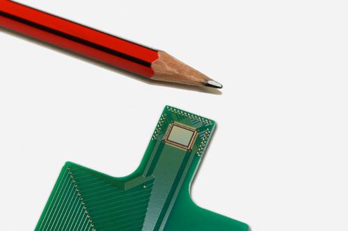
If you’re feeling a sense of deja vu right now, it’s understandable. The top plate is eerily reminiscent of that of the earlier Wi-Fi smart bulb, complete with an antenna (see the PCB-embedded traces?) sticking out the top. Note, too, the two odd prongs sticking out, one to the left of the labeled test points (which double as the power feed from the main assembly beneath to the LEDs), the other in the upper right corner of the Bluetooth antenna (we’ll circle back to those in a bit).

Remove two screws and the top plate pops right off.

No thermal paste bond to the metal sarcophagus underneath this time:


About that sarcophagus … from past experience, I knew that the only reliable way to get inside was to find the seam:

A flat head screwdriver-as-chisel, a Black and Decker Workbench, and a few taps from a hammer later, the deed was done (absent, I’m proud to say, any blood loss this time!):

No insulating black rubber surrounding the main assembly this time, interestingly:


The PCB slid right out, actually (note the mounting “brackets” on either side of the interior, intended to hold the PCB in place):

Whereas in past LED light bulb teardowns, the connection between the PCB and the base had comprised two flimsy wires, this time the implementation consisted of a more robust male-female connector pair plus a tension-tethered side terminal:


I’ll wrap up with some more main assembly closeups:


With that, I’ll turn the microphone over to you, dear readers, for your insights in the comments!
—Brian Dipert is Editor-in-Chief of the Embedded Vision Alliance, and a Senior Analyst at BDTI and Editor-in-Chief of InsideDSP, the company’s online newsletter .
Related articles :
Teardown: Wi-Fi LED light bulbTeardown: Zigbee-controlled LED light bulbTeardown: What killed this LED bulb?Teardown: A19 LED bulbHands-on review: GE Bluetooth smart light switchesAn LED ‘Filament’ Bulb: Not a ContradictionTeardown: Google’s Home MiniIoT connectivity: Wi-Fi and Bluetooth are winningTeardown: Smart switch provides Bluetooth power controlTeardown: Bluetooth由Voice of the EngineerLEDSColumn releasethank you for your recognition of Voice of the Engineer and for our original works As well as the favor of the article, you are very welcome to share it on your personal website or circle of friends, but please indicate the source of the article when reprinting it.“Teardown: Bluetooth”