Navitas’ design journey in the GaN semiconductor realm
- ICDesign
- 2023-09-23 23:01:42
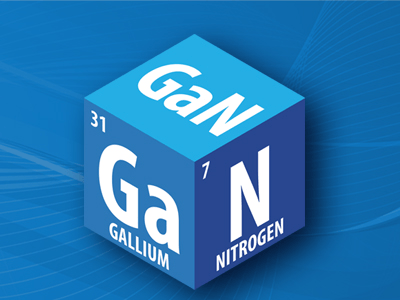
Navitas Semiconductor, a major gallium nitride (GaN) power device supplier, showcased its latest offerings at CES 2023 in Las Vegas. These GaN-based devices spanned from 20-W mobile phone chargers to 2-kW data center power supplies and 20-kW electric vehicle (EV) chargers to megawatt-scale grid-tied products.
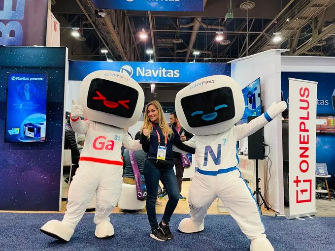
Figure 1 At the company’s booth, each presentation was followed by attendees having the chance to win prizes and giveaways. Source: Navitas Semiconductor
On CES 2023 floor, Navitas created some GaN buzz through presentations from its senior executives and GaN technology partners. The company was also able to highlight its “Electrify Our World” theme while announcing a variety of prizes for booth visitors. Navitas, meaning energy in Latin, has come a long way since being founded on a trailer in the parking lot of Hughes Research Laboratories (HRL) in Malibu, California.


It was founded in 2013 by former International Rectifier (HRL) executives Gene Sheridan and Dan Kinzer. The next year, investment firm MalibuIQ licensed the GaN power electronics technology from HRL, which had done significant work in maturing GaN devices for the military’s RF and millimeter wave applications.
In July 2015, Navitas raised $15.1 million in equity financing. It also moved from trailer to El Segundo, California, eventually setting up its headquarters in Torrance, California. The company currently employs around 200 people; about half of them are in the United States, and the rest are in different parts of Asia and Europe.
GaN design challenges
CES 2023 floor was a good place to gauge the design progress that GaN semiconductors have made over the past years. According to Dan Kinzer, Navitas co-founder and chief technology officer, the lack of high-performance circuits to drive the GaN transistors quickly and cost-effectively has been a key limitation for the potential of GaN semiconductors.
Navitas found a way around this design challenge via the monolithic integration of GaN drive and logic circuits with GaN power FETs. This monolithic integration enables high-frequency power conversion and the ability to shrink passive components such as transformers, EMI filters, and output capacitors. That, in turn, facilitates solutions that can charge 3x faster in half the size and weight of old and slow silicon devices.

Figure 2 Highly integrated GaN ICs bolster power density while significantly reducing size and cost. Source: Navitas Semiconductor
Stephen Oliver, VP of corporate marketing at Navitas Semiconductor, further elaborated on this crucial design premise for GaN devices while talking to EDN at the company’s booth. He said that GaN has been a great material in helping create fast and efficient semiconductors, but it has one big problem: gate. It’s very delicate, and if you put too much voltage on it, it will break down. Therefore, when you have a switch with a vulnerable gate, you must put a lot of protection around it. And that takes up more space and design costs.
Moreover, Oliver warned, you still have a chance to get a voltage spike. So, you have to slow things down or even consider going back to silicon. “It’s a very dead-end avenue.” However, the integration of GaN switch, GaN driver, GaN regulator, GaN ESD protection diode, level shifting, bootstrap, under-voltage lockout, and current sensing leads to the creation of a strong, powerful GaN IC.
Thermal management has been another stumbling block for GaN semiconductors. “The good thing about GaN is that resistance is much lower than silicon, which allows you to develop a very small chip,” Oliver said. “The bad thing is that smaller chips have a smaller surface area, so thermal resistance to the outside world is reduced.” Therefore, design engineers must ensure that the GaN device doesn’t create much heat. “What we have done with our initial platform is use standard QFN package size,” Oliver added.
GaN’s power disruption
To overcome GaN-related design challenges, Navitas is also adopting a platform- or system-level approach. “It’s a new technology, so if you offer something running at 2 MHz to power system designers who are used to working at 50 kHz, they’ll need a little help,” Oliver said. “We create design platforms built around a how-to-do-it approach so that engineers can review necessary details like bill-of-materials.”
Navitas entered the GaN foray at a time when this wide bandgap (WBG) technology had crossed the bridge from academia to commercial use cases. Fast forward to 2023, this GaN specialist, while having partnered with TSMC for wafers and Amkor for packaging, is confident in its ability to continue offering GaN solutions that can displace silicon in power electronics.

Figure 3 After mobile chargers and data-center power supplies, EVs are one of the next frontiers for GaN power devices. Source: Navitas Semiconductor
Just a few years ago, people asked when GaN would happen. And now, when GaN is already here, it’s probably a bit late to join the GaN party. Navitas is one of the few GaN device specialists that are now part of this power electronics market disruption. The year 2023 will likely be about market penetration, and Navitas seems part of this race for the GaN riches.
Related Content
SiC and GaN: A Tale of Two Semiconductors“Navitas Presents” to focus on GaN at CES 2023GaN’s applications roadmap spotted at CES 2023The diverging worlds of SiC and GaN semiconductorsIntegrated GaN Half-Bridge Delivers MHz PerformanceNavitas’ design journey in the GaN semiconductor realm由Voice of the EngineerICDesignColumn releasethank you for your recognition of Voice of the Engineer and for our original works As well as the favor of the article, you are very welcome to share it on your personal website or circle of friends, but please indicate the source of the article when reprinting it.“Navitas’ design journey in the GaN semiconductor realm”