-
Create high
Don’t spend years developing a NoC in-house. Increase productivity, reduce risk and speed time to ma...
 2023-09-23 23:01:30 191
 -

Simulation software gains embedded antenna models
Direct links to simulation models for 13 of Kyocera AVX’s embedded antennas are available in Ansys H...
2023-09-23 23:01:29 305 -

4 basic considerations in migrating to cloud
Here are four key factors chip designers should consider when turning to cloud-based EDA tools and s...
2023-09-23 23:01:29 121 -
A GaN technology reality check from the APEC 2023 floor
What took the center stage at APEC 2023 was gallium nitride (GaN)'s place in the quickly evolvi...
2023-09-23 23:01:28 151 -

Industrial MPU enables EtherCAT
The Renesas RZ/T2L microprocessor employs the EtherCAT communication protocol to provide high-speed ...
2023-09-23 23:01:28 309 -

APEC 2023: SiC moving into mainstream, cost major barrier
Silicon carbide (SiC), which complements silicon in many applications, is now enabling new power sol...
2023-09-23 23:01:27 149 -

Silicon carbide’s wafer cost conundrum and the way forward
Wafer cost, defects, scalability of device area, and ruggedness concerns were called major barriers ...
2023-09-23 23:01:26 253 -

Arm's prototype chips: What it means for the IC industry?
Arm is building prototype chips to demonstrate the power and capabilities of its IPs and designs to ...
2023-09-23 23:01:25 117 -

EDA toolmakers prep for TSMC's N3E and N2 nodes
The trio of large EDA houses are onboard and here is a synopsis of their undertakings to prepare for...
2023-09-23 23:01:24 226 -

Aspired European Nvidia aims DPUs at embedded AI
The IP-CUBE project led by Kalray aims to establish the foundations of a French semiconductor ecosys...
2023-09-23 23:01:23 283 -
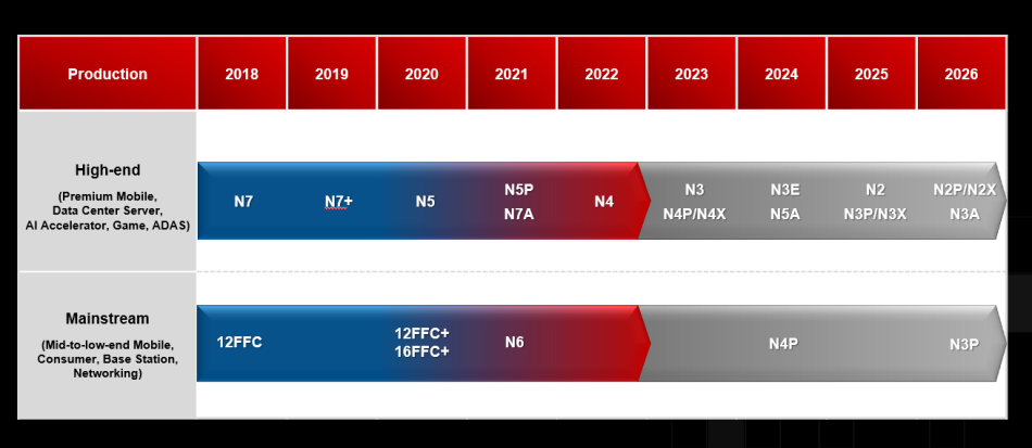
TSMC adds two variants to 2
Taiwan’s mega-fab will add two variants to its N2 technology in 2026: N2P with backside power delive...
2023-09-23 23:01:23 153 -

TSMC upends 3
The mega-fab’s 2023 North America Technology Symposium has provided ample information on the latest ...
2023-09-23 23:01:23 144 -

A brief history of gallium nitride (GaN) semiconductors
Here is how scientists and engineers overcame odds and made GaN workable first for LEDs and RF desig...
2023-09-23 23:01:22 250 -

Japanese fab Rapidus on the roll to catch up on 2
Rapidus, Japan’s new semiconductor fab, will acquire gate-all-around (GAA) technology from IBM to ma...
2023-09-23 23:01:21 150 -

4 technologies that sum up imec’s sub
Here is a sneak peek into the major process nodes and transistor architectures serving sub-1 nm with...
2023-09-23 23:01:21 245 -

A GaN technology breakthrough claimed for hard switching
A new IP enables GaN transistors in high-voltage, hard-switching applications to run at frequencies ...
2023-09-23 23:01:21 239 -
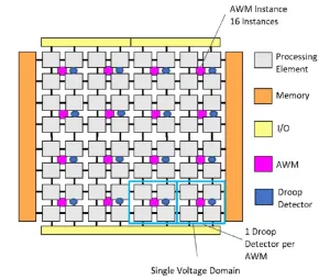
Droop response system IP made available for SoC designs
The off-the-shelf IP incorporates extensive monitoring and observability features to facilitate valu...
2023-09-23 23:01:20 205 -

Chiplets advancing one design breakthrough at a time
Multi-die chiplets are becoming critical in compute-intensive applications in data centers, cloud co...
2023-09-23 23:01:20 117 -

SoC design: When is a network
A system-on-chip (SoC) design can easily feature a combination of multiple NoC topologies to achieve...
2023-09-23 23:01:20 200 -

AI features in EDA tools: Facts and fiction
Artificial intelligence (AI) technology is still in its infancy, not just for EDA but for virtually ...
2023-09-23 23:01:19 292
Hot
-
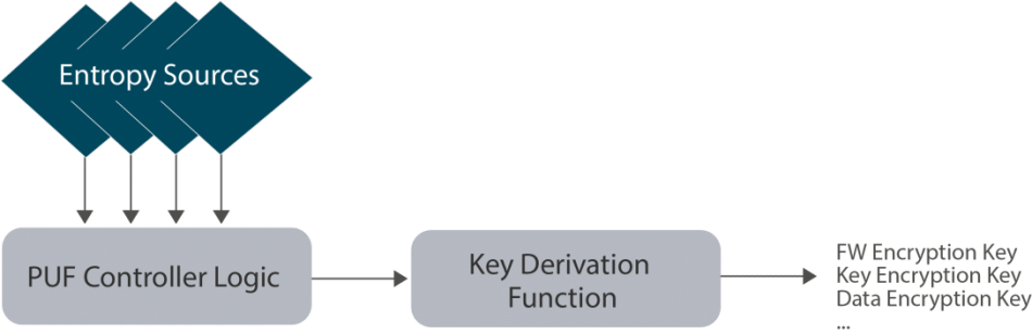
PUF update: New IP bypasses the need for ID enrollment
2023-09-23 23:01:35 -
APEC 2023: SiC moving into mainstream, cost major barrier
2023-09-23 23:01:27 -
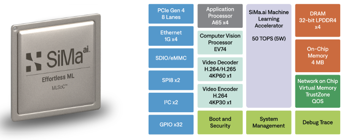
Vision processors bring AI to intelligent cameras
2023-09-23 23:01:31 -
Test
2023-09-23 23:01:45 -
4 technologies that sum up imec’s sub
2023-09-23 23:01:21 -
AI features in EDA tools: Facts and fiction
2023-09-23 23:01:19 -

IP partnerships stir the world of FPGA chiplets
2023-09-23 23:01:16 -

Why wafer cleaning matters in chip design and production
2023-09-23 23:01:18 -

Network
2023-09-23 23:01:17 -

A closer look at security verification for RISC
2023-09-23 23:01:39